alpha300 Semiconductor Edition
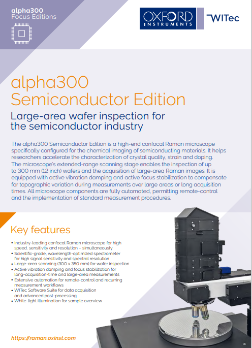
Large-area wafer inspection for the semiconductor industry
Discover the transformative capabilities the alpha300 Raman microscope brings to semiconductor wafer inspection:
- High Precision and Automation: Fully automated for high-speed, sensitive, and precise large-area measurements.
- Comprehensive Material Compatibility: Ideal for conventional and novel semiconducting materials, including 2D materials and heterostructures.
- Innovative Imaging Techniques: Features like TrueSurface technology ensure sharp imaging across entire wafers.
- Diverse Applications: From large-area wafer inspection to in-depth analysis of 2D materials.
Unlock the latest advancements in semiconductor material inspection by downloading the detailed report.
White Paper from 
If your Download does not start Automatically, Click Download Whitepaper